- 您现在的位置:买卖IC网 > Sheet目录518 > SQ4942EY-T1-GE3 (Vishay Siliconix)MOSFET DUAL N-CH 40V 8SOIC
SQ4942EY
www.vishay.com
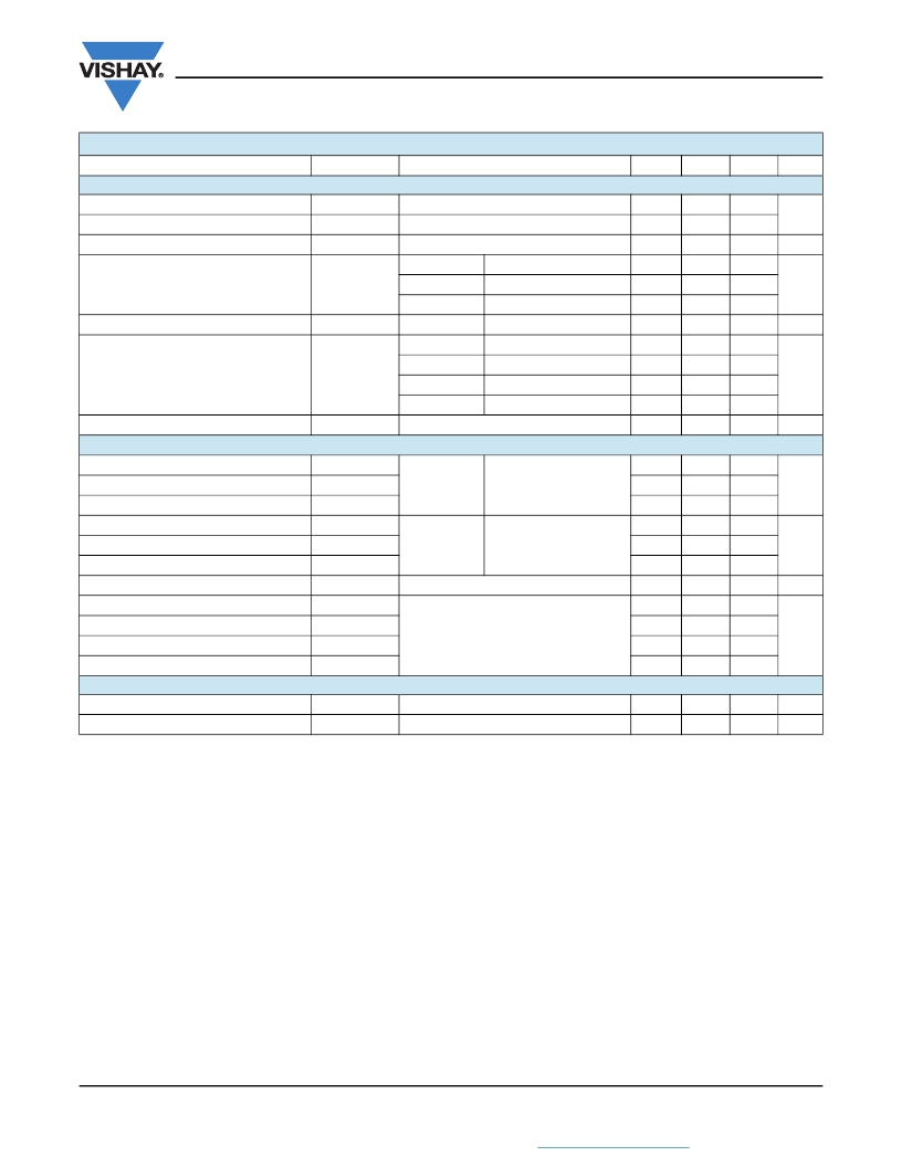
SPECIFICATIONS (T C = 25 °C, unless otherwise noted)
Vishay Siliconix
PARAMETER
SYMBOL
TEST CONDITIONS
MIN.
TYP.
MAX.
UNIT
Static
Drain-Source Breakdown Voltage
Gate-Source Threshold Voltage
Gate-Source Leakage
V DS
V GS(th)
I GSS
V GS = 0 V, I D = 250 μA
V DS = V GS , I D = 250 μA
V DS = 0 V, V GS = ± 20 V
V GS = 0 V
V DS = 40 V
40
1.5
-
-
-
2
-
-
-
2.5
± 100
1.0
V
nA
Zero Gate Voltage Drain Current
I DSS
V GS = 0 V
V DS = 40 V, T J = 55 °C
-
-
50
μA
V GS = 0 V
V DS = 40 V, T J = 175 °C
-
-
150
On-State Drain Current a
I D(on)
V GS = 10 V
V DS ??? 5 V
20
-
-
A
V GS = 10 V
I D = 6 A
-
0.016
0.020
Drain-Source On-State Resistance a
R DS(on)
V GS = 10 V
V GS = 10 V
I D = 6 A, T J = 125 °C
I D = 6 A, T J = 175 °C
-
-
-
-
0.031
0.036
?
V GS = 4.5 V
I D = 5 A
-
0.020
0.026
Forward Transconductance b
g fs
V DS = 15 V, I D = 6 A
-
23
-
S
Dynamic b
Input Capacitance
C iss
-
1409
1760
Output Capacitance
C oss
V GS = 0 V
V DS = 25 V, f = 1 MHz
-
199
250
pF
Reverse Transfer Capacitance
Total Gate Charge c
C rss
Q g
-
-
112
28.4
140
43
Gate-Source
Charge c
Q gs
V GS = 10 V
V DS = 20 V, I D = 5.7 A
-
4
-
nC
Gate-Drain Charge c
Q gd
-
6
-
Gate Resistance
Time c
Turn-On Delay
Rise Time c
Turn-Off Delay Time c
Fall Time c
R g
t d(on)
t r
t d(off)
t f
f = 1 MHz
V DD = 20 V, R L = 3.5 ?
I D ? 5.7 A, V GEN = 10 V, R g = 1 ?
0.5
-
-
-
-
-
8
13
20
9
2
12
20
30
14
?
ns
Source-Drain Diode Ratings and Characteristics b
Pulsed Current a
I SM
-
-
30
A
Forward Voltage
V SD
I F = 1.8 A, V GS = 0 V
-
0.75
1.1
V
Notes
a. Pulse test; pulse width ? 300 μs, duty cycle ? 2 %.
b. Guaranteed by design, not subject to production testing.
c. Independent of operating temperature.
Stresses beyond those listed under “Absolute Maximum Ratings” may cause permanent damage to the device. These are stress ratings only, and functional operation
of the device at these or any other conditions beyond those indicated in the operational sections of the specifications is not implied. Exposure to absolute maximum
rating conditions for extended periods may affect device reliability.
S11-2113-Rev. C, 07-Nov-11
2
Document Number: 65374
THIS DOCUMENT IS SUBJECT TO CHANGE WITHOUT NOTICE. THE PRODUCTS DESCRIBED HEREIN AND THIS DOCUMENT
ARE SUBJECT TO SPECIFIC DISCLAIMERS, SET FORTH AT www.vishay.com/doc?91000
发布紧急采购,3分钟左右您将得到回复。
相关PDF资料
SQ7414EN-T1-E3
MOSFET N-CH 60V 5.6A PPAK 1212-8
SQ7415EN-T1-E3
MOSFET P-CH 60V 3.6A PPAK 1212-8
SQD15N06-42L-GE3
MOSFET N-CH 60V 15A TO252
SQD19P06-60L-GE3
MOSFET P-CH D-S 60V TO252
SQD23N06-31L-GE3
MOSFET N-CH D-S 60V TO252
SQD35N05-26L-GE3
MOSFET N-CH D-S 55V 30A TO252
SQD40N04-10A-GE3
MOSFET N-CH D-S 40V 42A TO252
SQD50N02-04-GE3
MOSFET N-CH D-S 20V 50A TO252
相关代理商/技术参数
SQ4946AEY
制造商:VISHAY 制造商全称:Vishay Siliconix 功能描述:Automotive Dual N-Channel 60 V (D-S) 175 ?°C MOSFET
SQ4946AEY-T1-GE3
功能描述:MOSFET 60V 7A 4W RoHS:否 制造商:STMicroelectronics 晶体管极性:N-Channel 汲极/源极击穿电压:650 V 闸/源击穿电压:25 V 漏极连续电流:130 A 电阻汲极/源极 RDS(导通):0.014 Ohms 配置:Single 最大工作温度: 安装风格:Through Hole 封装 / 箱体:Max247 封装:Tube
SQ4946EY-T1-E3
功能描述:MOSFET 60V 4.5A 2.4W 55mohm @ 10V RoHS:否 制造商:STMicroelectronics 晶体管极性:N-Channel 汲极/源极击穿电压:650 V 闸/源击穿电压:25 V 漏极连续电流:130 A 电阻汲极/源极 RDS(导通):0.014 Ohms 配置:Single 最大工作温度: 安装风格:Through Hole 封装 / 箱体:Max247 封装:Tube
SQ4949EY-T1-GE3
制造商:Vishay Semiconductors 功能描述:
SQ4953EY-T1-GE3
制造商:Vishay Semiconductors 功能描述:
SQ4957
制造商:SEMICOA 制造商全称:SEMICOA 功能描述:Chip Type 2C4957 Geometry 0006 Polarity PNP
SQ4957F
制造商:SEMICOA 制造商全称:SEMICOA 功能描述:Chip Type 2C4957 Geometry 0006 Polarity PNP
SQ4961EY
制造商:VISHAY 制造商全称:Vishay Siliconix 功能描述:Automotive Dual P-Channel 60 V (D-S) 175 ?°C MOSFET
